


The optical communications landscape is moving at an unprecedented pace. Driven by the global surge in artificial intelligence infrastructure, hyper-scale cloud computing, and next-generation telecommunications networking, data transmission demands have skyrocketed. To address these evolving industry requirements and power next-generation optical interconnect technologies, GigaDevice, a leading global semiconductor supplier specializing in Flash memory, 32-bit microcontrollers (MCUs), sensors, and analog products, has expanded its specialized optical communication MCU portfolio. By offering fully self-developed, highly integrated, and mass-production-ready solutions, GigaDevice now provides the foundational hardware needed to support both high-speed and low-speed transceiver designs.
As optical communication applications become increasingly specialized, the microcontroller is no longer a one-size-fits-all component. Modern hardware designs require an optimal balance of processing power, analog accuracy, and physical space optimization. This is where GigaDevice’s tailored silicon paths, such as the GD32E512 series, come into play—demonstrating how radical hardware integration can solve the modern optical transceiver controller bottlenecks.
1. The Shrinking Footprint: Space Constraints and PCB Miniaturization
The push for higher bandwidth has triggered an industry-wide PCB miniaturization trend. Standard transceiver form factors must maximize faceplate density on network switches, leaving zero room for bulky design layouts.
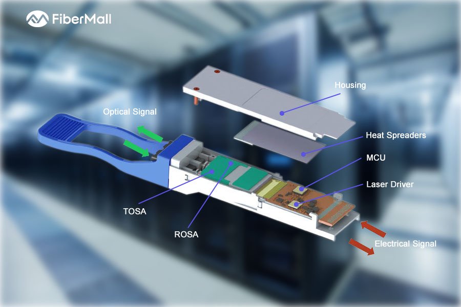
Inside a compact optical modules assembly, every square millimeter of printed circuit board (PCB) real estate is fiercely contested. The board must host high-speed optical components, laser drivers, clock and data recovery (CDR) chips, and the central controller.
When engineers rely on discrete layouts—using separate chips for processing, digital communication, and analog monitoring—the design quickly suffers:
l Trace Routing Complexity: Running dozens of high-frequency traces across a tiny board increases crosstalk risk and signal degradation.
l Component Clearance Bottlenecks: Placing multiple discrete packages close together violates physical manufacturing constraints and creates localized thermal hot spots.
l Parasitic Capacitance: Longer PCB traces between separate chips introduce parasitic resistance and capacitance, which can corrupt sensitive diagnostic readings.
2. GigaDevice’s On-Silicon Solution: The Power of Rich Analog Integration
To break free from these physical layout limits, GigaDevice has leveraged its comprehensive technology portfolio to evolve the modern integrated MCU far beyond its traditional role as a simple digital logic manager. Instead of forcing engineers to crowd a design with external monitoring chips, GigaDevice utilizes a consolidated mixed-signal architecture. By pulling critical analog components directly onto the microcontroller silicon, designers can completely eliminate an entire ecosystem of external support chips, resulting in a cleaner layout and significantly improved signal integrity.
Integrating specific analog peripherals brings significant, measurable structural advantages to modern optical module design:
Precision Telemetry via ADC and DAC
An optical transceiver relies on constant feedback loops to keep data streams clean. Multi-channel Analog-to-Digital Converters (ADCs) continuously track real-time telemetry, including internal operating voltages, laser bias currents, and received optical power. Concurrently, Digital-to-Analog Converters (DACs) translate digital instructions back into precise voltage thresholds to continuously calibrate laser performance and modulate transmission strength.
Fast Diagnostics via COMP and OPA
Laser monitoring requires instantaneous action. Integrated Operational Amplifiers (OPAs) condition low-amplitude sensor signals right on the silicon, preventing external noise from corrupting data. Meanwhile, integrated Analog Comparators (COMP) act as autonomous hardware tripwires. They monitor signal thresholds in real time and can trigger automated safety shutdowns or flags if a laser overcurrent occurs—all without waiting for the main CPU core to process a software interrupt loop.
Streamlined System Protocols via I²C and MDIO
A highly capable controller must talk to both internal components and external host systems efficiently. Built-in, hardware-managed communication ports like I²C and Management Data Input/Output (MDIO) enable clean, standardized diagnostic reporting. They handle configuration loops and host queries smoothly without requiring external interface conversion logic or heavy software emulation.
3. Tangible Advantages: Reliability, Efficiency, and Lower Bill of Materials
Transitioning to GigaDevice’s deeply integrated system design framework yields massive operational and economic benefits across the product life cycle:
l Drastic Component Count Reduction: Replacing external amplifiers, standalone digitizers, and communication chips with a unified MCU reduces the total Bill of Materials (BOM). Fewer components mean fewer parts to source, simpler supply chain logistics, and lower assembly costs.
l Enhanced System Reliability: Every solder joint on a PCB represents a potential point of failure due to thermal stress, vibration, or manufacturing defects. By consolidating multiple hardware components onto a single piece of silicon, engineers drastically lower total point-of-failure risks, maximizing the Mean Time Between Failures (MTBF).
l Accelerated Time-to-Market: Developing firmware for a unified, pre-verified internal hardware ecosystem is much easier than writing driver code to sync multiple discrete components from different chip vendors. This streamlined programming workflow slashes debugging times and helps engineering teams hit tight market windows.
4. Technical Implementation: The GD32E512 Integration Matrix
To address these rigid spatial constraints without compromising telemetry accuracy, the GigaDevice GD32E512 series consolidates a highly sophisticated hardware matrix onto a single silicon die. Powered by a high-performance Arm Cortex-M33 core running at 120 MHz, the microcontroller delivers substantial processing headroom while serving as a comprehensive mixed-signal hub.
For diagnostic precision, the device integrates dual high-precision ADCs for real-time telemetry logging, alongside four independent DAC channels that provide fine-grain control over laser voltage modulation. Instantaneous hardware protection and sensor conditioning are managed on-chip via two operational amplifiers (OPAs) and two analog comparators (COMPs), eliminating the need for external supervisory chips. Furthermore, host-side communication is streamlined through three I²C interfaces and a dedicated MDIO bus. By packing complete control, monitoring, and communication routing into an ultra-compact 3 × 3 mm package footprint, this application-optimized controller allows hardware designers to easily meet strict space-saving goals without overloading the tight physical constraints of the transceiver layout.
Conclusion
In modern optical module development, integration is no longer just a convenient design option—it is a foundational requirement to overcome strict space limitations, navigate PCB miniaturization trends, and hit next-generation performance targets.
By utilizing GigaDevice’s advanced application-optimized controllers, which pack vital analog, communication, and processing tools right onto a core chip, hardware engineers can eliminate external component dependencies. Embracing this level of hardware integration ensures that global optical networks remain fast, durable, and fully prepared for the massive data demands of tomorrow.
